Friday 27 April 2018

Do Hybrid Perovskite Solar Cells increased performance of Neutrons??


The fundamental mechanisms behind the conversion of sunlight into energy in hybrid perovskite materials is the neutron scattering. This behavior of the perovskite solar cells will enable manufacturers to design solar cells with significantly increased usage and efficiency.

To study the relationship between the material's microscopic structure and its optoelectronic properties scientists used photoluminescence measurements, along with neutron and x-ray scattering and establish how hydrogen bonding plays a key role in the material's performance to track atomic structural changes in any atom or crystals.
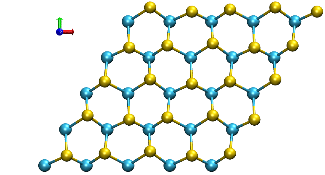

Neutron scattering show the orthorhombic structure of the hybrid perovskite cells that are stabilized by the strong hydrogen bonds between nitrogen substituent of the methylammonium cations and bromides on the corner-linked PbBr6 octahedra.

Hybrid perovskite cells are more easy and efficient in converting light into energy than solar cell materials. These cells are easier to manufacture as they can be spin cast from solution and do not require high-vacuum chambers for synthesis. Hybrid perovskite are made of both organic and inorganic molecules. Neutrons are sensitive to lighter elements like hydrogen that helps in finding the right combination and molecular orientation of the different organic/inorganic components. With the help of neutrons we are able to get information where the atoms are, their temperature, characterization and observe the hydrogen bonding interactions at the atomic scale. The experiment using the perovskite cells and crystals is done to observe how the organic molecules were binding to the lead-bromine component through hydrogen bonds.

This study reveals about the perovskite solar cells how sunlight is being absorbed and what tells the applications for photovoltaic materials. Photoluminescence and x-ray scattering measurements were performed to measure theoretical calculations of crystals along with crystal synthesis. Hybrid perovskites shows the orientation of the organic molecules that impacts the crystal structure and these different methods helps us to design new materials with even greater potential.

Meet us at “4th International Conference on Crystallography & Novel Materials” in Bucharest, Romania for more recent updates on Material Science, Crystallography and Nanotechnology.

For more details, contact:
Jessica Mark
Program Manager | Crystallography Congress 2018
Tel: +1-201-380-5561 Ext: 7008
Toll No: +44-2088190774


Friday 20 April 2018

Atomic force microscopy (AFM): Graphene-Based Electronics


A straightforward method to adjust atoms in a single bearing on a level graphene surface and effectively controlling sub-atomic arrangement is depend upon to prompt real advance in surface science and sub-atomic designing and above all in the field of materials science.

Graphene is a type of material that is attracting many scientists, students and researchers as a powerful candidate for next generation of electronics materials and in the field of material science due to their unique properties. The graphene surface has three-overlay symmetry, which are thermodynamically equal to each other and along these lines making it hard to adjust the atoms in an arranged or special course.

Atomic force microscopy (AFM) is a type of technique mainly used for detecting surfaces additionally to control sub-atomic arrangement and produces pictures demonstrating the surface uneven layer of precious stone by sliding a test tip over the surface region.


The grey plane represents the graphene surface. The stick-like particles consisting of white, grey, red, yellow white colored balls represent surfactant (sodium dodecyl sulphate (SDS)) molecules. The grey colored reverse pyramid-like structure shows the probe tip of AFM.

At that point the examination on AFM, it demonstrates how AFM tip filtering prompts changes in atomic arrangement on the graphene surface of any material or precious stone. They utilized sodium dodecyl sulphate (SDS), a typical surfactant atom, as a model particle and it forms like ribbon on the graphene surface. It has been observed that SDS strips developed effectively when the relative edge between the ribbon developing hub and the sweep bearing is bigger and adsorbed SDS atoms are really evacuated when they are compelled to pivot under the AFM filtering conditions. This method shows that the AFM scan can help in the 'symmetry breaking' effect of the molecular pattern on graphene.


The idea of breaking the surface symmetry can be used for different purposes, for example, producing sub-atomic circuits in sub-atomic hardware science as well as in related fields that include sub-atomic nanostructures and their arrangement.

Meet us at “4th International Conference on Crystallography & Novel Materials” in Bucharest, Romania for more recent updates on Material Science and Crystallography.


Friday 13 April 2018

Machine learning: Designing Chiral Crystals


Logistic regression is a statistical method that can tell apart two objects and is also compared it to use in smartphones. In face recognition, smartphones use machine learning to classify faces and things that are not faces, so we can train our model to detect chiral and non-chiral possibilities, but here the input is not an image, its information."

Chirality describes the quality of possessing a mirror image to something else, but without the ability to superimpose it. Your left foot, for example, is a mirror of your right. They look similar, but they are not the same.

In chemistry two molecules can have the same makeover of elements, but still they differ in their geometry, also a left-handed chiral helix can have a corresponding to the right-handed helix.

But, making a mirror image of a chiral molecule is more difficult than just simply rearranging some bonds and is more complex when making a crystal, in this case a highly arranged series of atoms or molecules exist in three dimensions.

The scientists analysed about the crystals that there are 686 chiral crystals and 1000 achiral crystals from the most recent Inorganic Crystal Structure Database by using the technique logistic regression. Logistic regression analysis model predicts ideal chiral crystal also used to predict which chemical groups are best for making chiral molecules and also used to calculate which chemical groups of the periodic table have elements or atoms that are more likely to coexist in a chiral crystal and the groups that correspond to carbon, nitrogen, and oxygen are the best with group numbers 14, 15, and 16 respectively.

The most interesting and difficult part of making a chiral crystal are to know how to design them; it is difficult to mix different atoms so that their chiral geometry coexists in a single crystal. From this chiral crystal we can predict crystals and explore how to build a chiral magnet from them.

To get the latest updates and share your thoughts on Crystal growth and Crystallization - Join us for the advance Talks/Sessions at Crystallography Congress 2018.


For more details contact:
Jessica Mark
Program Manager | Crystallography Congress 2018


Friday 6 April 2018

Optical communications: Silicon-Chip Graphene Blackbody Emitters


The rapid light producers that are incorporated on the silicon chips can help in novel designs for making silicon-based Optoelectronics. In spite of the fact that, the compound-semiconductor-based light producers see diverse real difficulties for the coordination with the silicon-based stage because of their trouble of creation on the silicon substrate. Utilizing the rapid and exceptionally incorporated graphene-in light of silicon-chip black body producers in the Near-Infrared (NIR) district the media transmission wavelength was created and utilized.

Here the square of multiple graphene sheets are connected to the source and drain electrodes, then the modulated blackbody emission will be produced from graphene by giving the input signals.
Graphene is a two-dimensional Nano carbon material, having unique properties in electronic, optical and thermal properties, which can be applied for optoelectronic devices. Graphene-based black body emitters are the emerging light emitters on silicon chip in Near-Infrared (NIR) and mid-infrared region.

The emission responses can be controlled by the graphene contact with the substrate depending on the number of graphene layers. The mechanisms of these are given by performing theoretical calculations and methods of the heat conduction equations using the thermal model of emitters including both graphene and a substrate.

Graphene light producers are extraordinarily invaluable over traditional compound semiconductor producers since they can be exceedingly incorporated on silicon chip because of basic manufacture procedures of graphene producers and direct coupling with silicon wave guide through a transient field. The graphene-based light producers can open new courses to exceedingly coordinated optoelectronics and silicon photonics.

The latest researches on Material Science and nano material can be known at 4th International Conference on Crystallography & Novel Materials to be held during November 19-20, 2018 at Bucharest, Romania.

Crystallography Congress 2018 is a 2-day event offering wider sessions involving Keynote presentation, Oral, YRF (student presentation), poster, e-poster presentations.

Contact:
Jessica Mark
Program Manager | Crystallography Congress 2018